

Application
Contact Us
Guangdong Yinchuang Technology Co.,Ltd.
Tel: +86-138 2925 8465Email: [email protected] [email protected]
Add: No.229 Shuixin Road, Fumin Induistrial, Dalang Towm, Dongguan City, Guangdong Province, China 523000
Semiconductor
viewing count: 4693Release time: 2022-04-14
體點膠噴嘴.jpg)
Semiconductor packaging technology, a microchip contains tens of billions of transistors, criss-crossed links and orderly work, whether it is Kirin 990 or Snapdragon 855, the combination is the score and speed, semiconductor assembly is a complex splicing process , it is necessary to control each section of the process well in order to obtain a good and stable product. Chip encapsulation, BGA chip underfill, solder joint encapsulation, wire reinforcement, die bond, component fixation and other dispensing operations play a key role in the stable work of semiconductors.
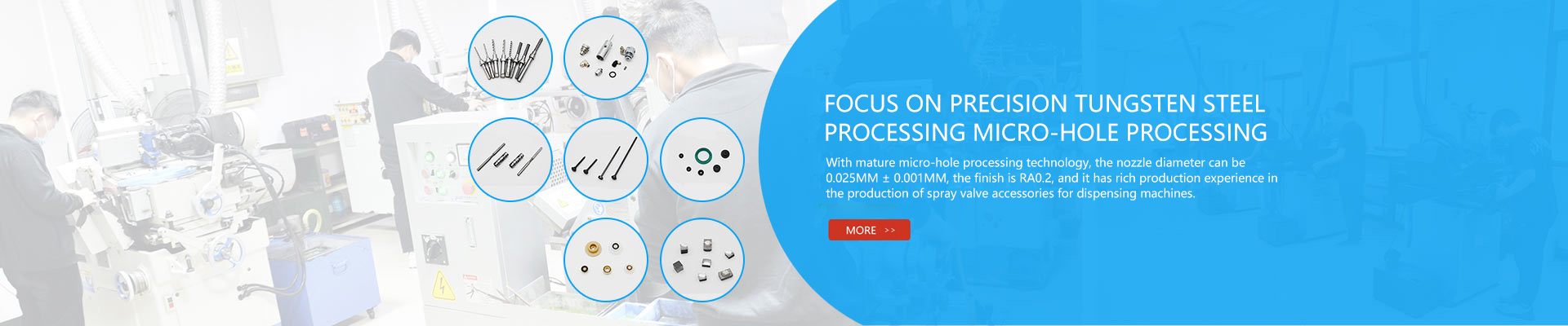
As the needs of the small chip dispensing process, we provide Die Bonding Tools ( Epoxy Stamping Tools , Micro Dispensing Nozzle , Pick-up Tools , Ejector Needles)
Glue Volume 20μm-600μm
High quality finishing on precise micro holes
Perfect round holes , hole cylindricity controlled
Tolerance ±1μm
Material: tungsten carbide, ceramic , stainless steel
